DIY Module Front panels (two questions and a big tangent)

Not a real update, but an interesting thingy that I bought by mistake (I wanted to buy KR140UD12 which is one of the OpAmps needed for a Polivoks filter that I am considering to make using all the original stuff), anyway by mistake I ordered a B140UD12A. And it turns out, this thing is just a core of an OpAmp, no body, no pins. Just a core and thin-thin leads. It was very cheap too (20 rubles. That’s about 33 cents, I think). I don’t think I can use it, sadly. Look!

That’s all for now!

1 Like

The Polivoks filter looks like an interesting design, this is my first time reading about them, my apologies but I am unable to read most of the documentation due to my lack of Russian language skills, I did find a web page with a design I could read. It would appear the original design used no capacitors or inductors, so if I get the time it’s a circuit I would like to understand more about, but not sure if / when I will get around to it.

I can’t really tell from the picture, but what you have looks like some form of surface mount component. I have still not used these, as I am an old hobbyist with poor eyesight and a fear of having to learn how to solder these, but many hobbyists do with success, and good old youtube has enough videos on the subject to send even the greatest insomniacs to sleep.

I am not sure if you have found the correct component yet, but Polivoks VCF shows some alternatives that can be used. Alongside the original schematic, there is an alternative design designated clone, that has input and output buffers to match the signal levels used in a eurorack ish design.

Most opamps used in synth designs cost less than a dollar, and if you are designing your own layouts two TL072’s can be replaced by a single TL074 in most cases and would work fine for the input and output buffers in this design, but I would stick with the recommended alternatives for the KR140UD12 .

On a more light hearted subject, how is the cat you showed at the start of this post :slight_smile:

1 Like

The image shows what the inside of a chip in a can , DIP or flatpack looks like. The thin wires are ultrasonically welded to the chip and to the external pins.

2 Likes

Thank you, I have never seen this before, I had mistaken it for a standard I was not familiar with.

Out of curiosity, is there a use for the shown component, outside of the semiconductor industry, I am wondering why it is possible to purchase these as single items?

Well, coming from a semiconductor manufacturing background, those fine wires were never designed to be user solderable. You would probably destroy any chip if you try to solder to it. Otherwise, I don’t know.

1 Like

I think there is an interview somewhere with the guy that invented this filter. Maybe it is translated or… well, if it is a text, it is google-translatable anyway, haha.

Oh, it’s easy to find, actually. But it costs more than TLs, like 6 times more. Because there’s gold or platinum there… And also the package is different, It’s in the UFO body as I call it, not the rectangular black thing, but a flying saucer round thing. And with my anxiety it’s a torture. Cause I would have to check the leads 100 times before even before soldering it (it’s round and the leads are not marked properly, there’s a notch or something that indicates the first lead as I remember). And after that I would check it 100 times again. And still there would be a possibility of mistakes. Right, so I will do it eventually, and with all the original stuff, also including resistors and transistors. Gladly it works at around 12v, so it perfectly matches my PSU setup (I don’t even know why there’s a 15v DIY standart, is it louder? More precise? Or just because?).

Yeah! It’s funny though that at the shop where I am buying the electronic stuff TL072 costs just as much as TL074 does. So there’s a difference between two 72s and one 74! I mean, price-wise.

Hahaha. I have a lot of drawings like this! And a real cat… Her name is Mathilda and she’s a black cat with eyes very similar to godzilla’s.

1 Like

Yep! That’s what I also deduced. To me it’s more like a curiosity or something. An object. But…

Is there really no way? Like if I try to somehow use it… Maybe soldering while cooling the chip? Or maybe there’s no real danger of overheating it? I was thinking it would make a cool design. Like if I use this chip in a circuit and also make a window for it in the front panel of the module… With LEDs maybe… But it’s not like I am seriously considering it. Not yet!

I do not think you can solder to the “lead” wire that is ultrasonically welded to the chip. But you could probably solder to the other end of the lead wire.

1 Like

Ah, yes! By the way. I think it could be used in some kind of more complex ICs. And here I am, in the middle of this chain. OR it could be for the selling purposes. Like look how cool our chip is! There’s also almost (except for this weird datasheet (in russian, sorry)) no info on this in the internet. A mystery!

1 Like

Aaah. Well, that’s what I was thinking about. I am not this bold to try and solder the wires to the chip itself… So Yeah, I was thinking about connecting it to the PCB with some kind of wires and a pin header… Or just soldering it directly to the PCB, I am not sure yet. It’s a fun thing though! I really like how it looks. Like an alien device!

2 Likes
		// scheme to chop blue on dark modes
		// keeps things normalized and highlights feedback
		// and the "LOGO"
		switch(kind) {
			case INPUT_PORT:
				textColor = SCHEME_GREEN;
				break;
			case NORM_KNOB: case SNAP_KNOB:
				textColor = SCHEME_YELLOW;
				break;
			case OUTPUT_PORT:
				textColor = SCHEME_RED;
				break;
			case GR_LED: default:
				textColor = SCHEME_BLUE;
				break;
		}

and

        // Textual Name Display
	// an ego-logo-ism of blue tint when the lights are down
	// on the star trek there is always enough pupil to see the wonders of space
	// classic human interaction design
	// cyan panels, yep, plenty of light mode wake up there
	// plenty of intense green and wakey blue
	display = new LabelWidget(named, GR_LED);
	display->fixCentre(locl(lanes / 2 + 0.5f, 0.5f), strlen(named));//chars
	m->addChild(display);

I thought you posted it by mistake at first, haha. So that’s how you program a front panel, right? It’s cool and interesting! But this thread is about physical DIY modules and real physical front panels. Probably I should’ve mentioned it in the name of this thread… But anyway! Thanks, it might help some people searching for this info!

1 Like

It’s plugin 2 development, learnt from the fix up and play with colour variety.

Another small update with possibly great implications

So @Curlymorphic gave me a link to Rich Holmes YT channel and a video dedicated to transistor matching. That’s what this thing does. I made it using the original schematic (by which I mean the one from the Ian Fritz’s paper) with the original modification: I added a trimmer to match the resistors.

Sorry that this photo is a bit dark. It is dark, but look how good the quality is! Wow!

So what about these great implications? Well, for once it is the actual function of this device: now (I hope) I can match the transistors and assemble VCAs and stuff. I think some filter schematics need this too… And even some VCOs. Anyway, very useful thing! One problem though: my multimeter is pure shite. And it just became even less good. It is relatively new, I bought it maybe 3 months ago, and it already started to act strangely. The thing that you turn to change the settings, like a position switch or whatever you call it, it makes a weird noise. And when you actually try to measure something, it just walks about indecisively, maybe it is 100k, or wait, it’s 98k, ah sorry, 100,8k. Nah, just kidding, 99k! And it doesn’t stop after a while like you would expect. So I ordered another DMM that should arrive today. This one is bigger! Bigger is better, right? Anyway, this old multimeter despite how bad it is, gave me a present! An unexpected one.

So to explain what it was, I have to draw something!

The idea was to roughly set a trimmer, in other words to equalize the resistance between X1 and OUT and X2 and OUT. So I started with measuring the X1 to Y1 resistance, just in case, and it was surprising. It should be 100k, right? Well, plus or minus 1% and shiteness of my DMM. But the result was 23k. Okay, what does X2 to Y2 says? 56k. That can’t be right. If there was a solder bridge or something, it should show me 0 ohm. But there can’t be a solder bridge anyway, the schematic is very simple! As you can see on the pic, I haven’t attached the 3rd pin row to the ground yet. It was just a bridge between 3rd pin and 6th pin. No connection to anything. So I measured the resistance between Z1&2 and X1&2 and it was about 60k both times. I checked some other places on the PCB and somewhere it was 70-80k of resistance even though there wasn’t anything there. My first thought was that the PCB is bad. Maybe the layers somewhere inside got damaged and the solder somehow filled this space. But! It seems the flux I use is conductive. And that’s one part of the problem. Another thing is that my solvent doesn’t solve my problems! On the package it says: “Can be used for flux removal” or something, but it could be that it doesn’t wash it completely. But a week ago I bought a liter of pure isopropanol. I wasn’t using it yet, cause I had this other solvent. Right, so I washed the PCB with the isopropanol and it helped a lot!

So what are the implications, how it changes anything? Well, I already told yous about my experience with LFO that behaves weirdly and I also told yous about my problems with pink noise. This problem was so bad I had to redo the plan, cutting out the pink noise part from the schematic completely. And now we have a suspect! It could be that the flux residue screws everything up and my old solvent isn’t doing anything to prevent it. So I have to rewash everything I made and be aware for the future! And maybe I also have to change the flux. I wasn’t aware that it conducts electricity.

Here’s another cat to lighten the mood! He plays with a laser dot!

I read that as “UFO” and it made a lot of sense :wink:

3 Likes

This post shows so much progress, just look at how happy this cat is compared to the last picture.

I have found prototyping boards to be very fiddly when soldering. They don’t have the same solder mask as a pcb so it is much easier to bridge connections, and these bridges are sometimes not easy to see with the naked eye. A good scrub with an old tooth brush, and leave it to dry for a few hours, then scrub with a dry toothbrush to remove any loose excess can really help.

Yeah… Well, this one (I will call it PCB anyway, not a prototyping board, because it’s a pain to type it every time. SO “the green PCB”) is actually good compared to the red PCB that I also have. The problem with these red ones is that sometimes the pads are falling off after you heat them. But it was cheap! And I am a cheapskate.

Yeah, that’s exactly how I do that. Well, minus the dry toothbrush. I usually go with solvent+toothbrush and then a visual inspection, with a magnifying glass sometimes. I thought that’s enough, but it seems that I was wrong, haha

1 Like

TLDR.

About the panel material, how about transparent Lexan? (aka polycarbonate).

If you put mirror-image decal lettering on the back and then paint over that (“reverse-painting”), neither the paint nor the lettering will wear off. A lot of glass vintage radio dials were done that way.

1 Like

I was considering it too. But the only piece of polycarbonate I have is too small and I couldn’t seem to find a nice one to buy. The ones I found were… hollowed? I don’t know what they call them. Like this: image

I can buy a fine and more usefull list of polycarbonate online though. But it’s too late for this particular project. I might do it for the next project (but it would be much later, maybe in a year or more). Thanks though! The painting idea is very very cool!

Alright, so for the next module I decided to go with YASH, as I already said before. At first I was thinking about making a jfet sample&hold. Just because It seemed easier and… I don’t know, maybe I just love transistors. But after receiving J111 and experimenting with it a bit I realized that what I got is, probably, a fake jfet. It didn’t work like jfet at all. I was trying to make a simple circuit to check if this J111 is fake or if I am stupid and this one is real… BUT while thinking about it I just decided to go with Yash, which is also a very simple circuit. No way to mess it up, right? Hahaha. There are many ways to mess it up if you are me.

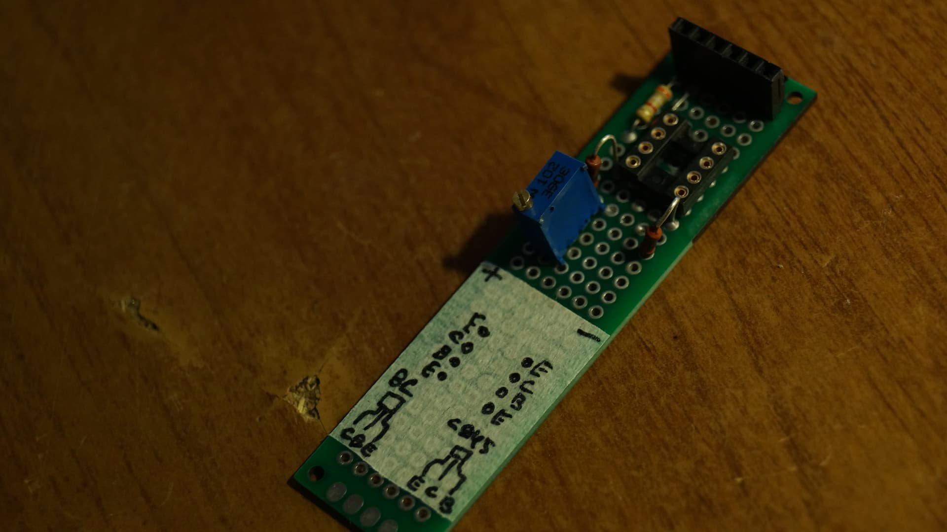
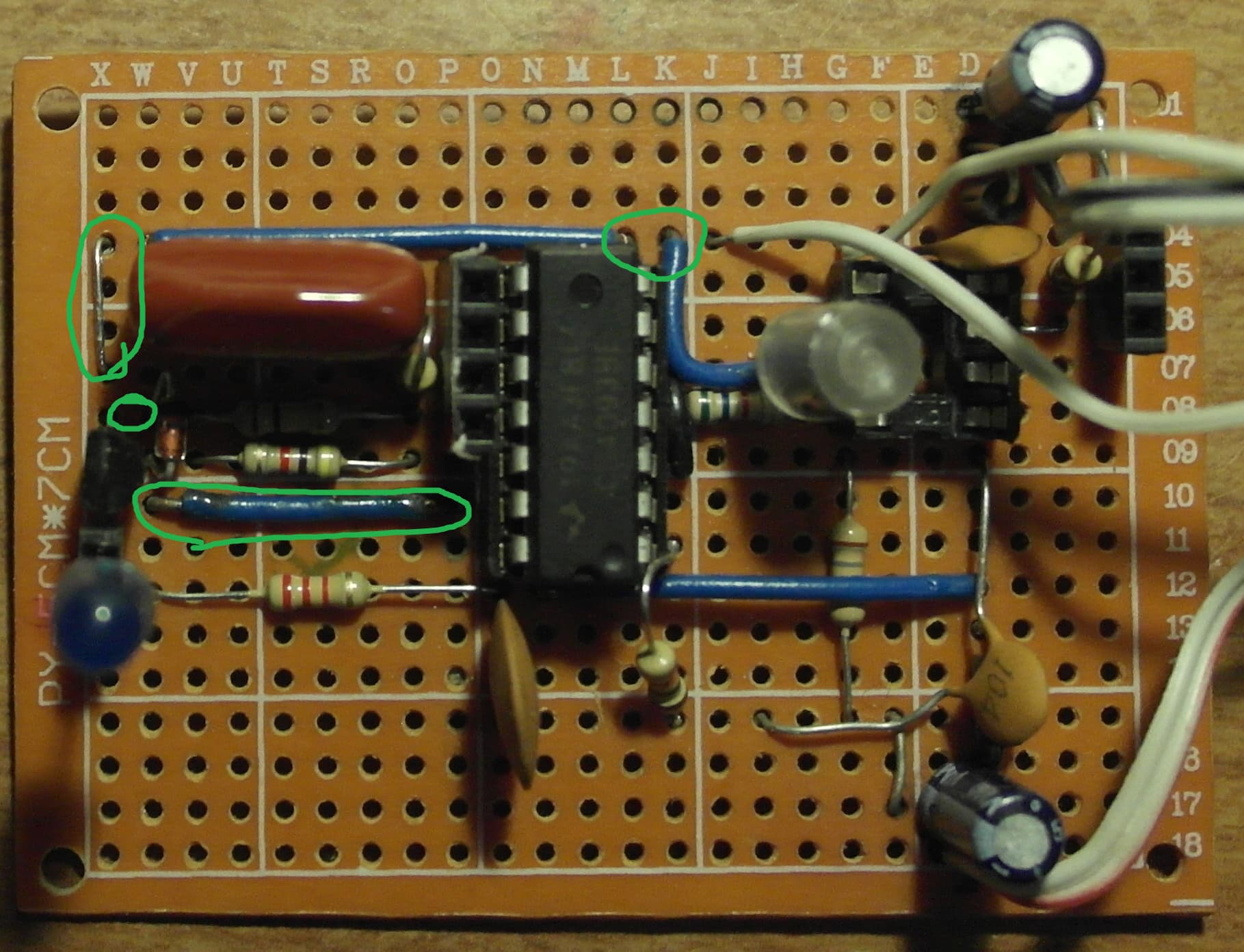
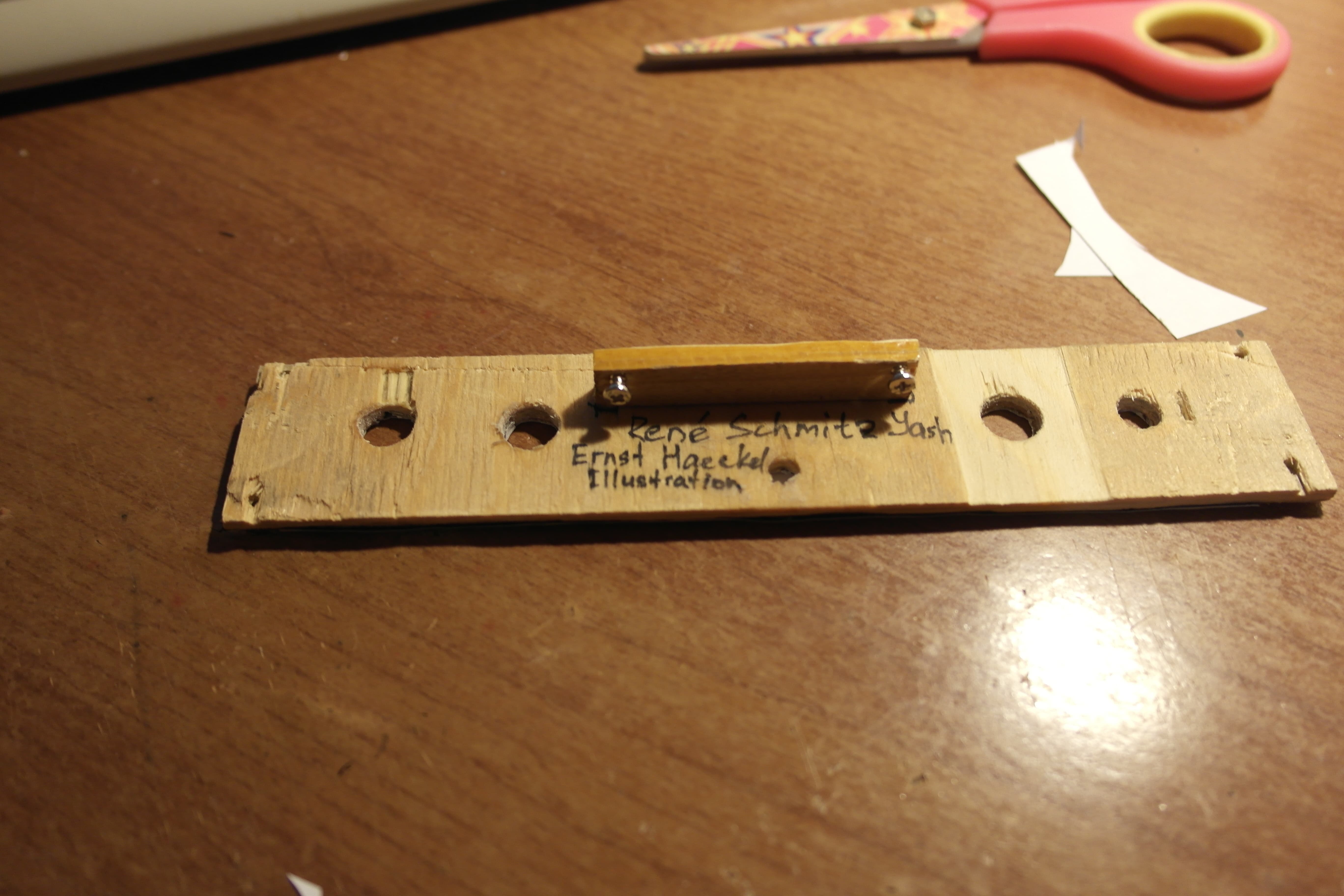
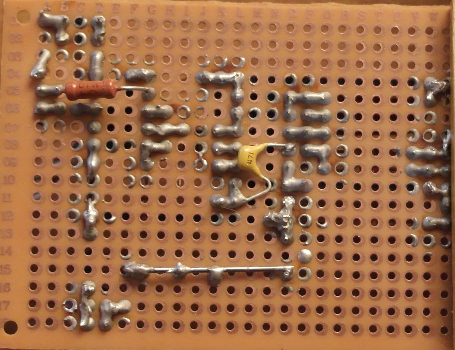
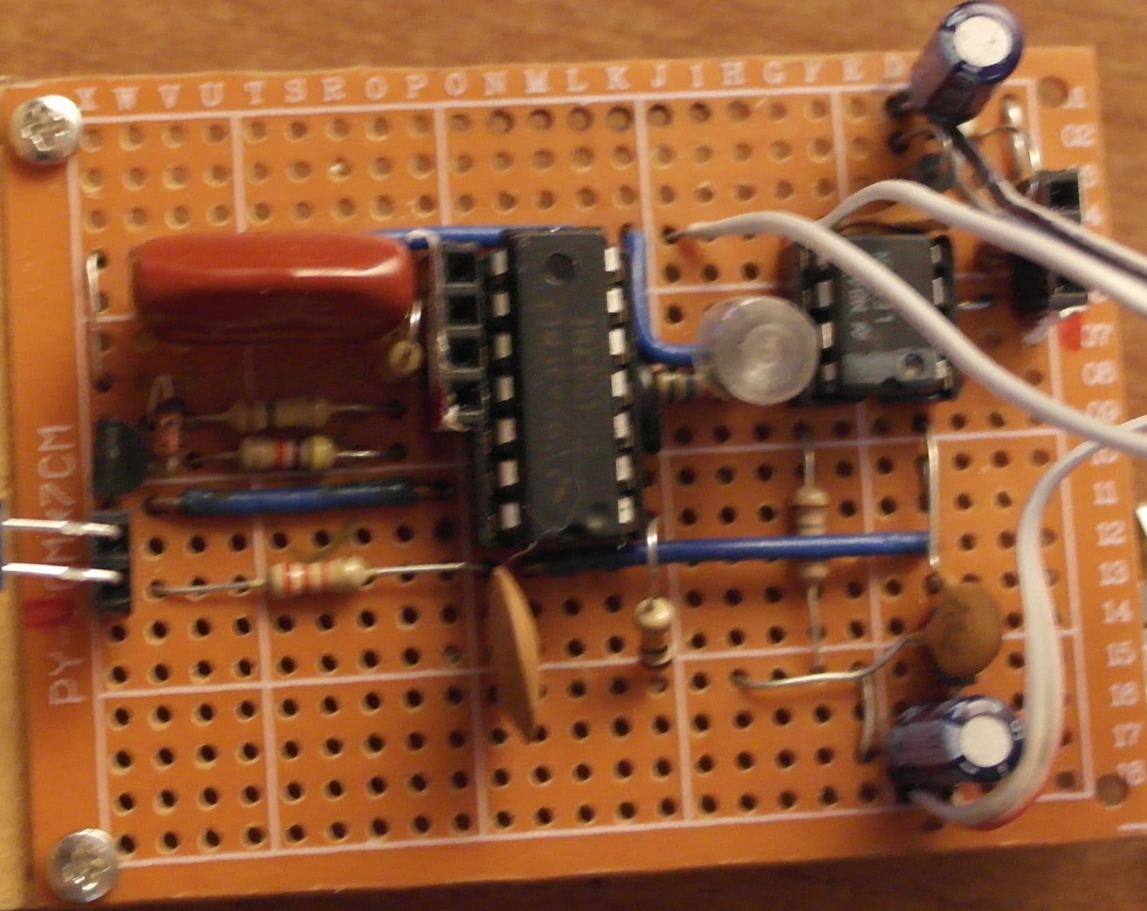
So look at the board. See the green marks? That’s all the places I forgot to add or solder together.

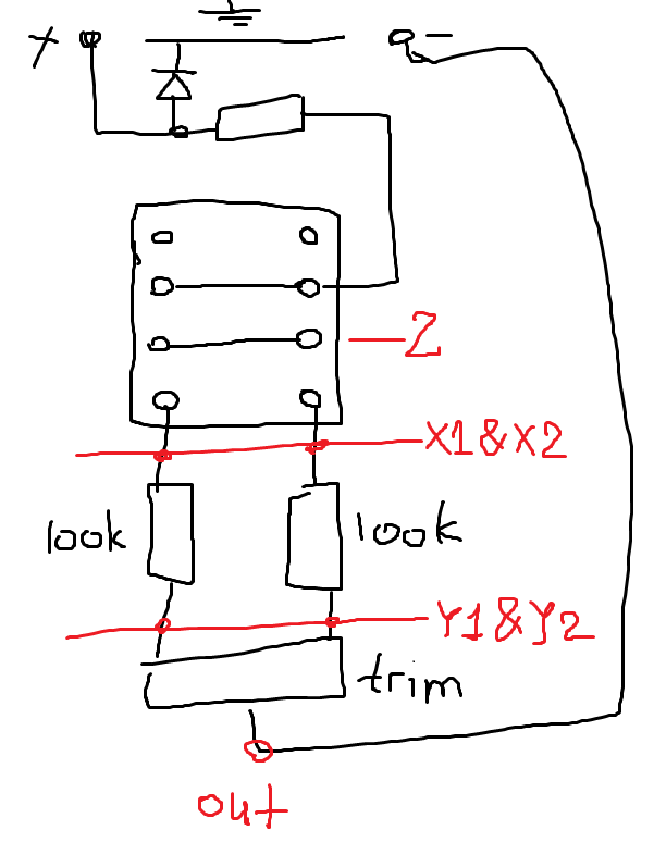
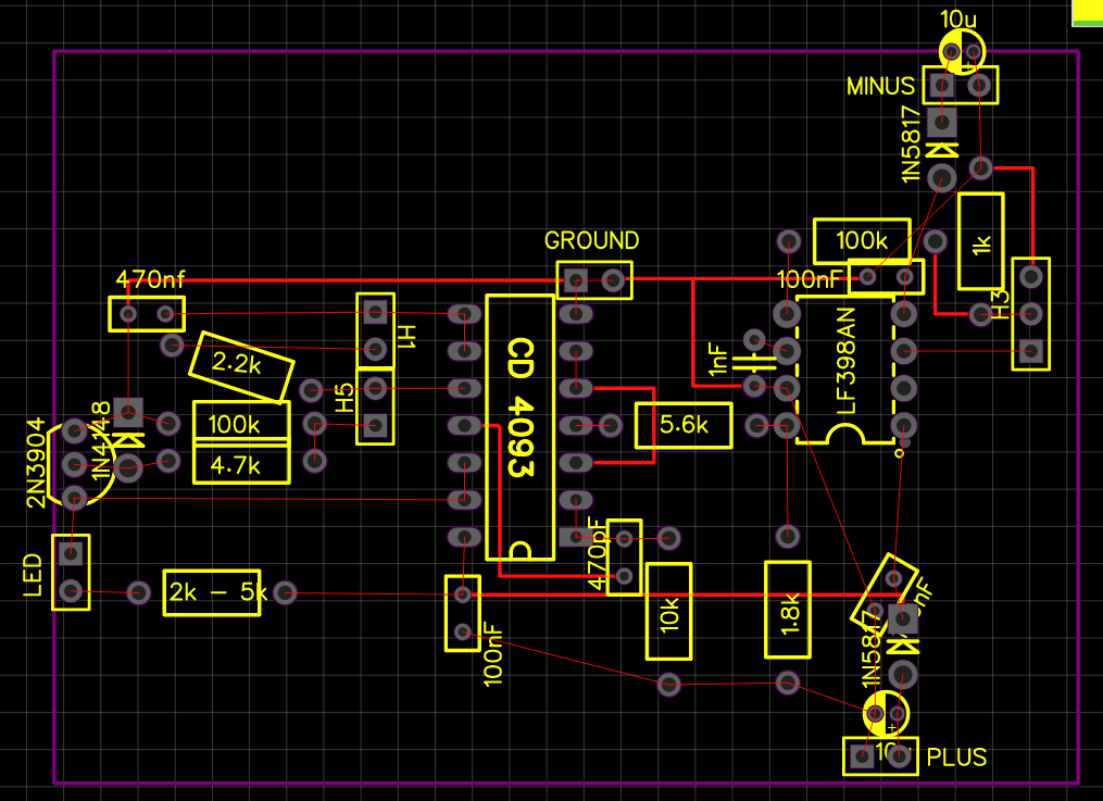
And it still doesn’t work for some reason. I don’t know what might be the problem here. I am 80% sure it should work now. But it doesn’t! While checking the circuit it appears that the pulse from the inner oscillator almost disappears before reaching the LF398 (which goes to the slot at the right side of the board). And if that’s not enough to make me depressed, something wrong with jack inputs/outputs too. My fault totally, I bought a big pack of cheap jack sockets. Well, I am sure this problem is solvable, even if I would have to destroy the socket, remodel it and put it back together again. The circuit, however, needs more attention, and I am not sure what’s wrong with it. Could be that I have a faulty CD4093, but that’s the only one I have, so I can’t just replace it to see what would happen… I also caught a very annoying cold and it makes it extra difficult to concentrate and check the circuit while looking at the schematic (which is mirrored and a bit different, because I was doing it at easyeda and it’s a pain to search for the footprints)

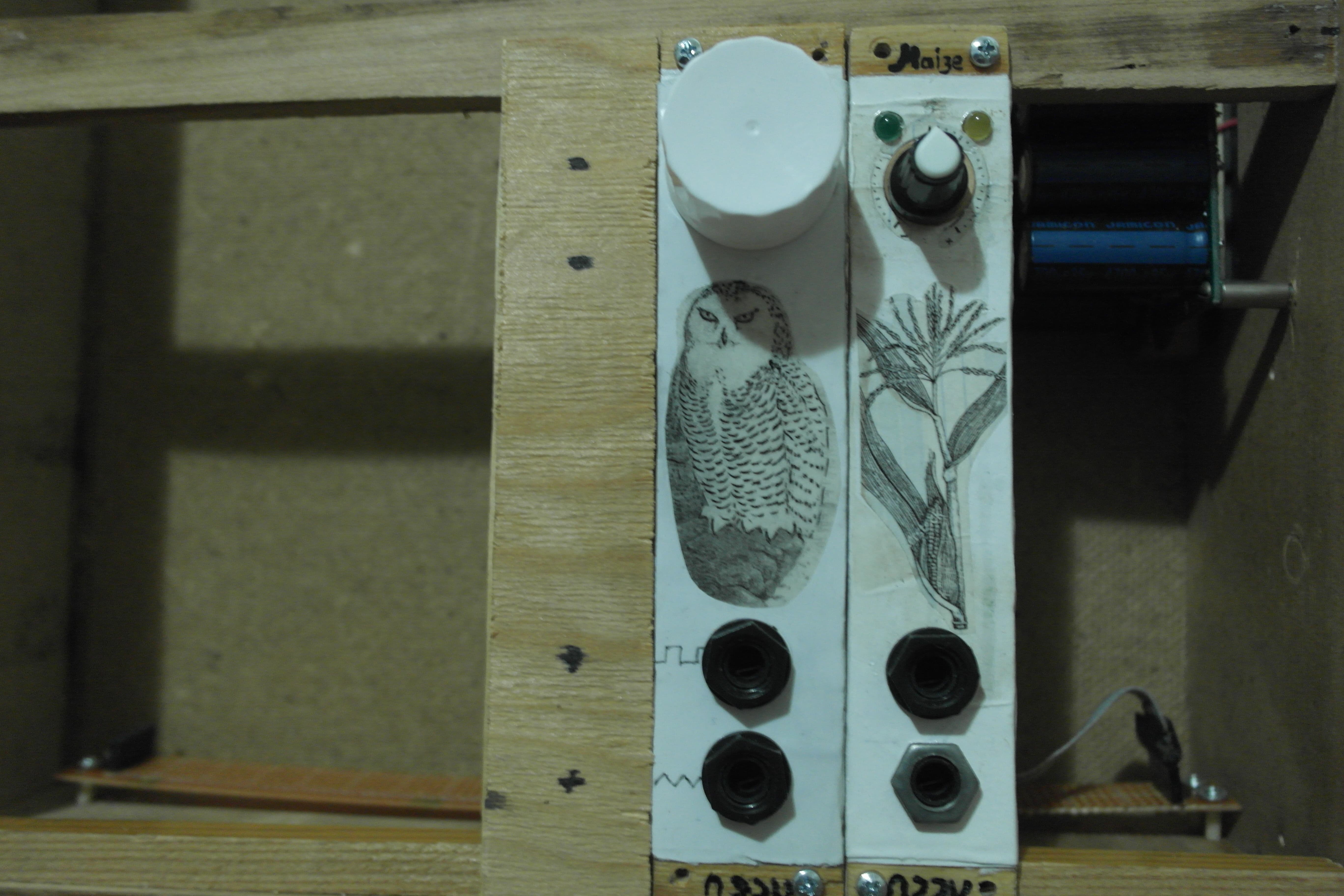
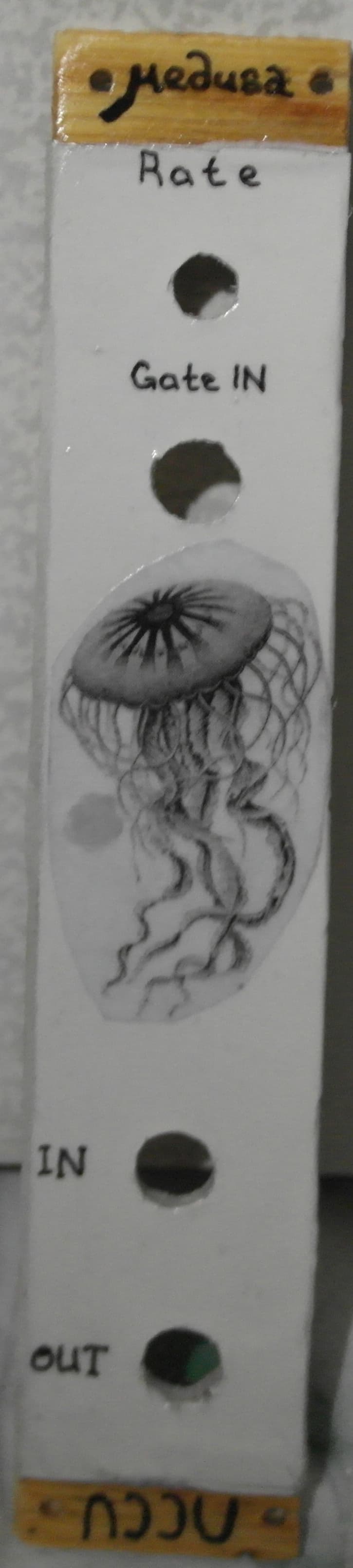
But as I started this thread with front panels, I must show you the front panel for this module. It is ready! Shame that module itself isn’t working… Alright, here’s my process. I already shared the photos, but let’s do it again!

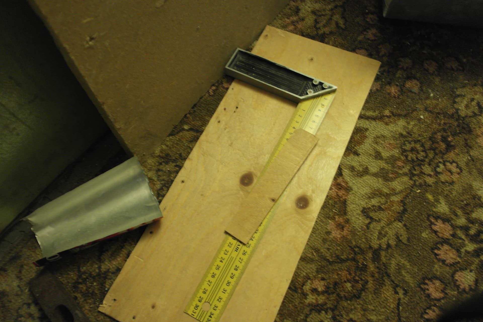
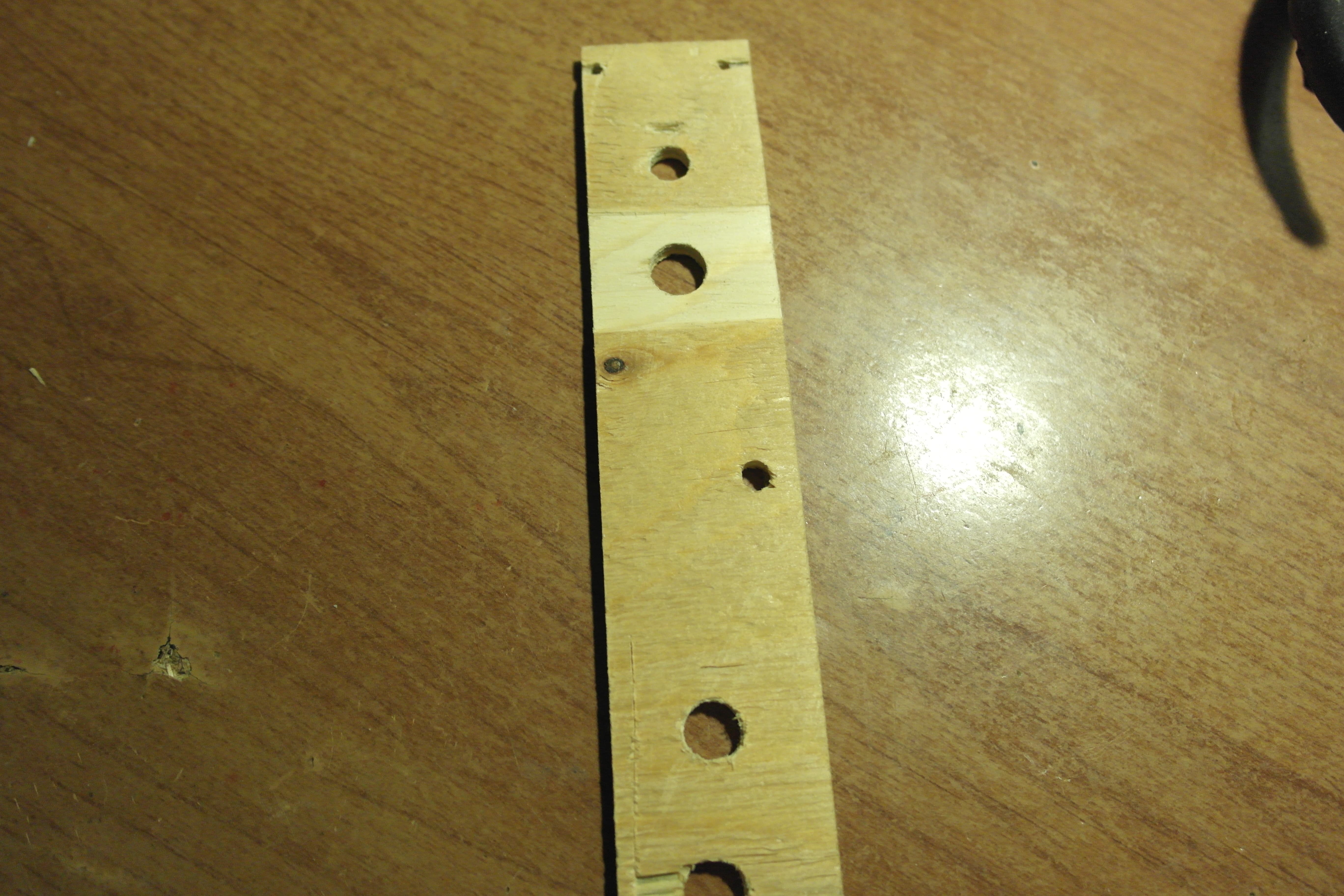
At first I cut a plywood. I don’t really care if it’s not perfectly rectangular, but I am trying to make it as good as it could be. I cut it with a knife, because it’s thin. And also it’s easier for me to use a knife than a saw.

Then I cut 1-2 cm from the upper/bottom side and place it with my other modules to see if it’s fine. If it is, I mark the screw positions (forgot to mark it here) and jack sockets positions and other stuff that I think I would need.

Then I usually measure it again, just to be sure that I wouldn’t encounter any problems with placing the panel elements and mark the markings, because unmarked markings are as confusing as this sentence.

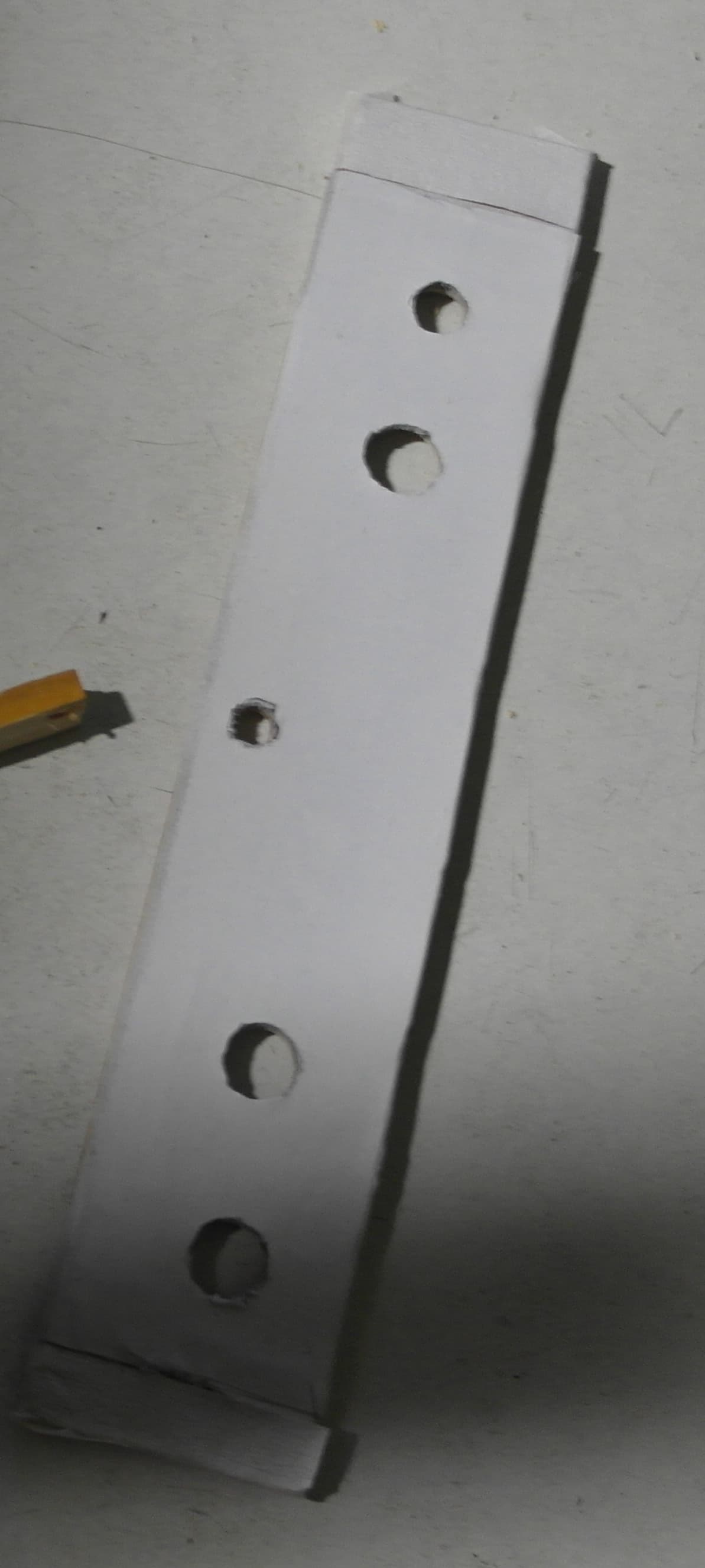
I drill holes and file the plywood, at the spots where I will place the jack sockets. I wish I had a filing machine or something. Hate it.

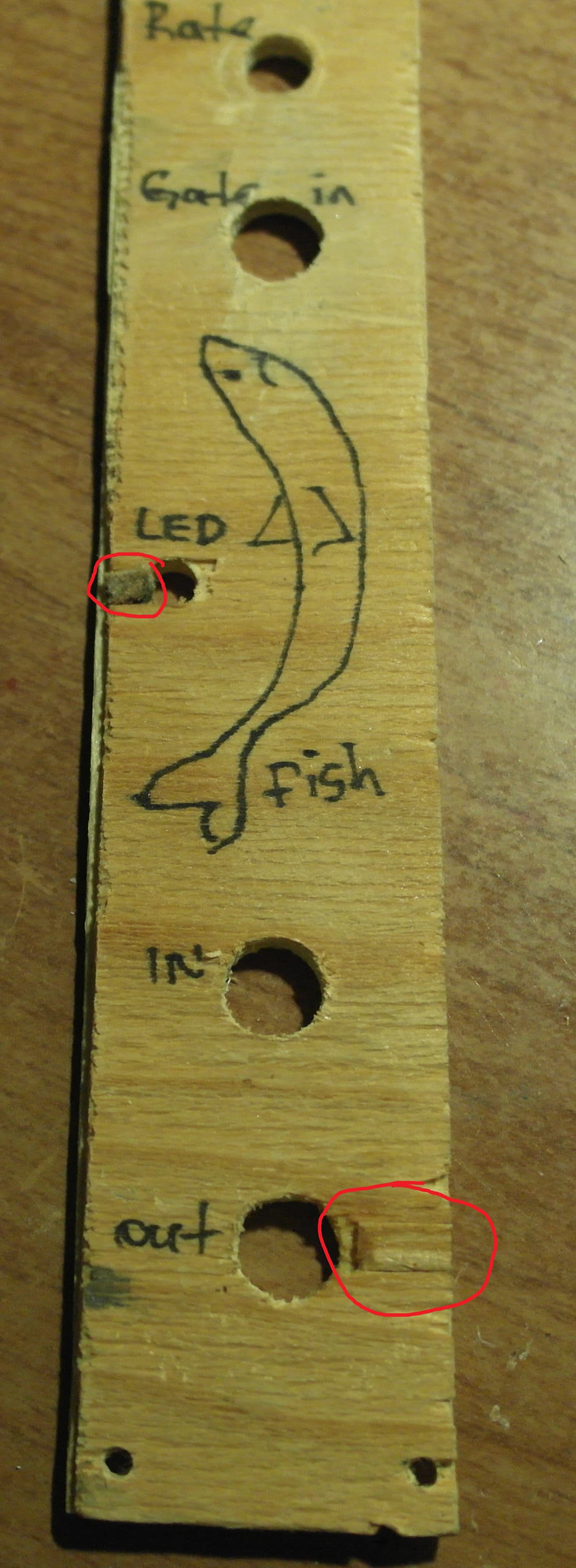
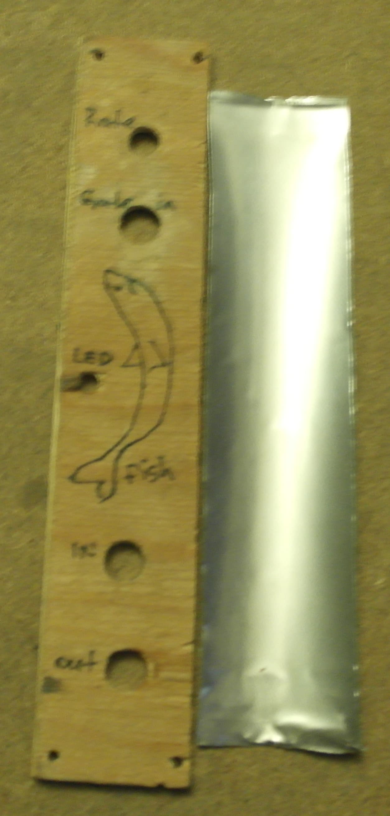
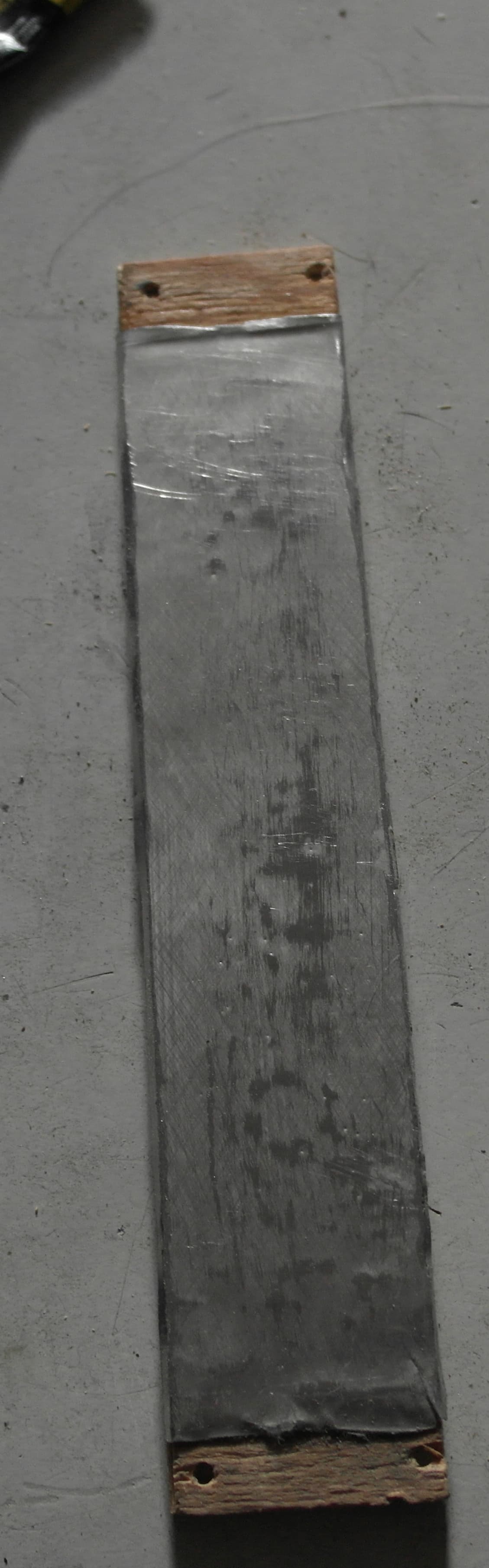
Then I glue the stuff that I damaged while drilling the holes. And after that I glue the aluminium “face” to the plywood.

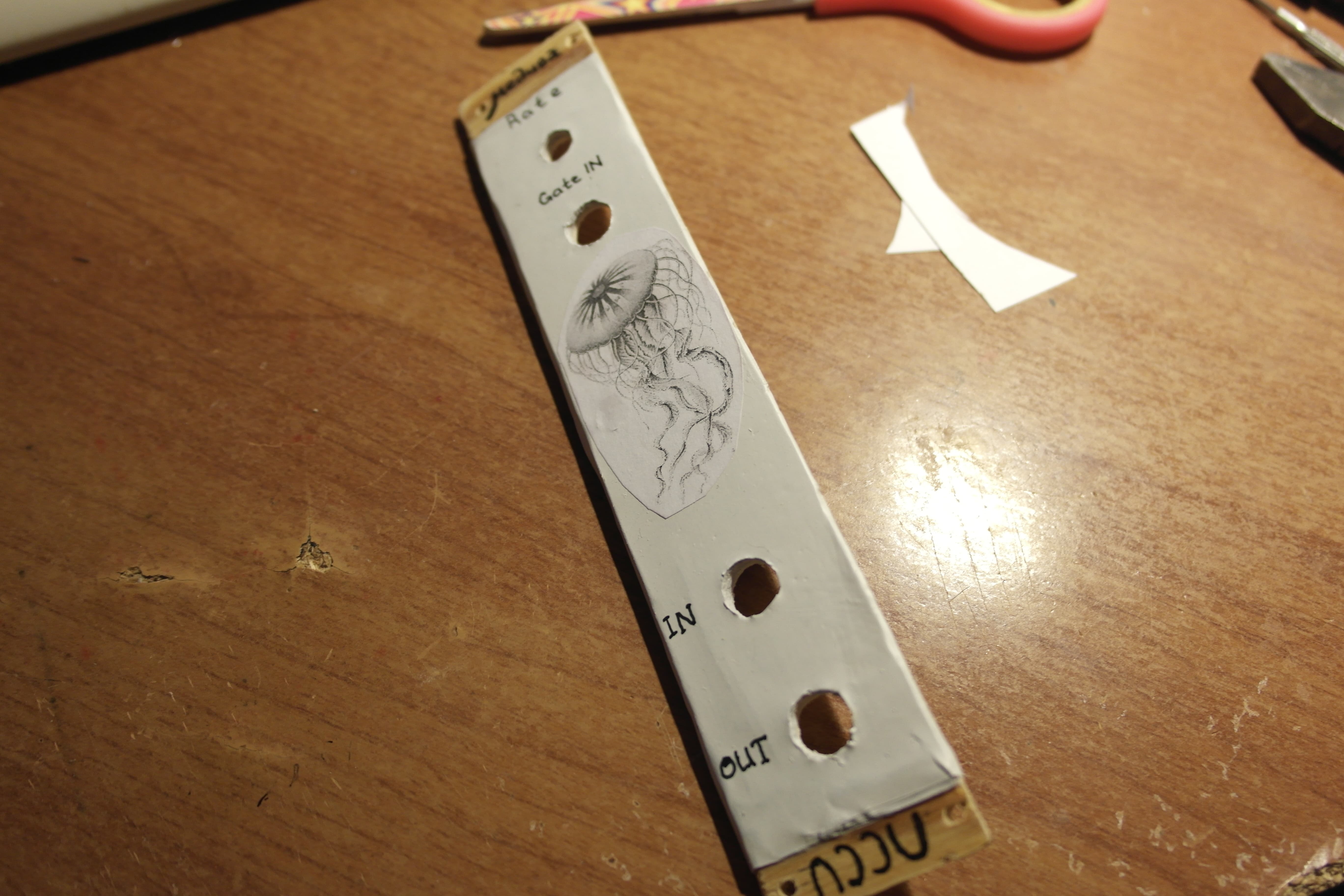
The finish line! I poke holes with a screwdriver and clean it with a knife, then paint it, et voila!

Then I add a pretty picture from the internet and write with a gel pen words like “IN” and “OUT” and all these user friendly interface elements. And at the back I write the name of the schematic and a name of an artist that made the illustration that I used

1-2 layers of lac and we’re ready!

Sadly I can’t show you how it looks when it works, because it doesn’t work. But I will try to fix it and then I will show you how cool it looks when blue LED light blinks! Super nice.

Anyway if you have any ideas what could be wrong with my schematic, I would appreciate it. I know that there’s not enough information, so here’s my eda project:

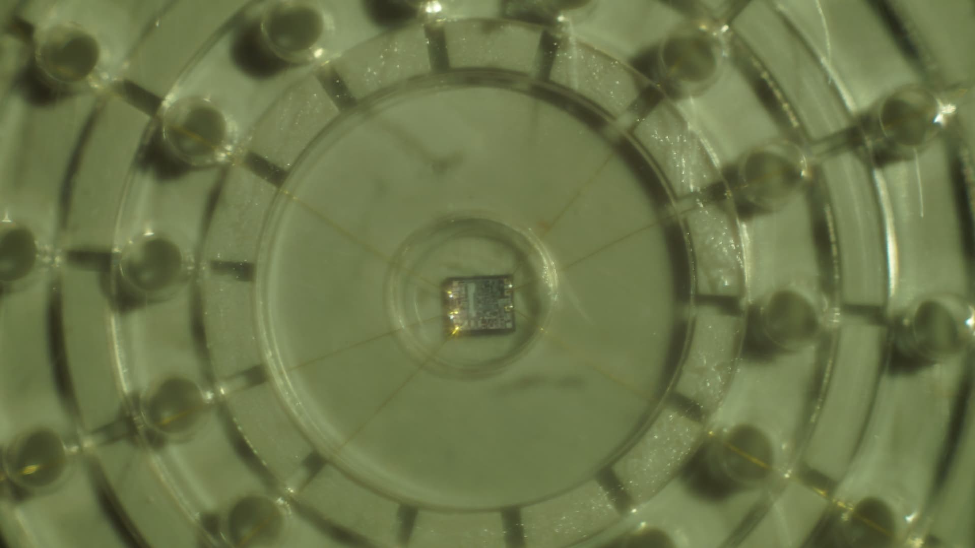
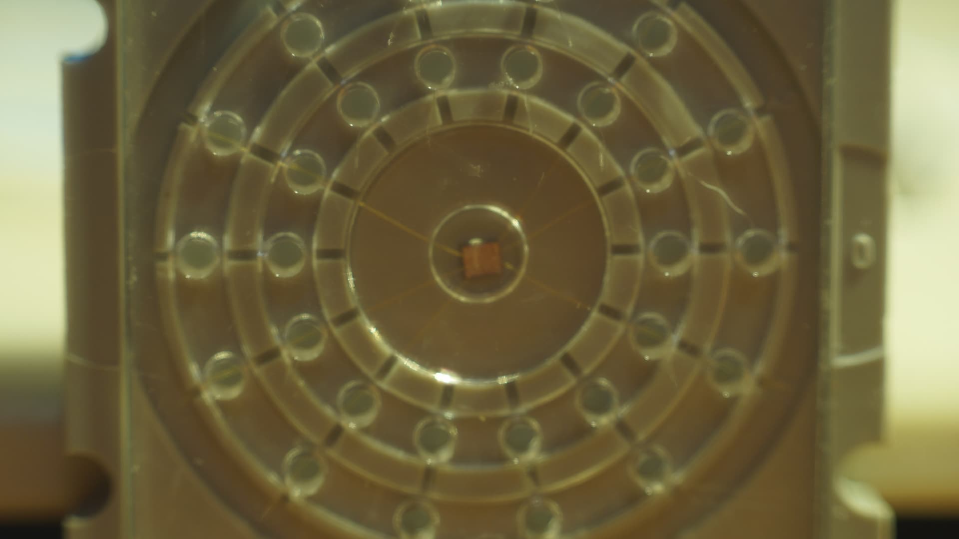
And both sides of a board:

I am not desperate yet, so it’s not like I am begging you to sit for an hour searching for what I did wrong, haha. But if there’s something obvious that you noticed right away, please let me know!